In this video, I want to talk about two different types of temporary memory, or RAM, that we use in FPGAs.
After introducing these memory types, I'll discuss when and under what circumstances you should use each type.
More...
The Role of RAMs in FPGA-Based Systems
Even if you have just a little experience in digital design, you know that when implementing a digital system, you often need to use temporary memory or RAM.
For example, in your circuit, there might be a portion of calculations whose results need to be used later in another part of the circuit. In such cases, you’ll need to store the results of that calculation in a temporary memory.
Or, maybe you're sampling data from an input, for example with an analog-to-digital converter (ADC), and you want to send that data out of the FPGA (perhaps to a computer or another FPGA) after the sampling is complete.
In that situation, you also need to store this data in temporary memory.
Another application where you might need temporary memory is if you want to store tables of coefficients or specific curves within the FPGA.
For instance, you might need to store one period of a sine wave in a table so you can use it to generate a sine wave within the FPGA.
Since temporary memory is commonly used in most digital designs, FPGAs come with built-in hardware blocks specifically designed for creating and managing memory.
Internal RAM Types in FPGAs
Generally, there are two types of memory in FPGAs: Block RAM (BRAM) and Distributed RAM.
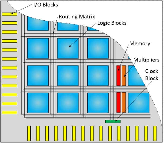
If you’ve watched the first video in this tutorial, you might remember this diagram. It shows the hardware resources available in an FPGA.

Diagram of the hardware resources available in FPGA.
As you can see, the red sections represent the Block RAMs. These are hardware blocks pre-built into different parts of the FPGA, which you can use as memory.
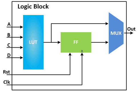
The blue sections represent the Logic Blocks. If you recall from a previous video, we explained that these blocks primarily consist of LUTs (Look-Up Tables).
LUTs are actually very small memory units that can be used to implement small circuits. By connecting multiple LUTs, you can design larger circuits.
With that recap, let’s dive deeper into what Block RAMs and Distributed RAMs are.
Block RAM (BRAM)
As I mentioned earlier, Block RAMs are hardware blocks pre-designed into FPGAs that you can use to implement temporary memory. These memories typically come in fixed sizes.
For instance, in Xilinx FPGAs, Block RAMs are often 18 kilobits or 36 kilobits in size, and there are a significant number of them available in the FPGA.
Each of these 18- or 36-kilobit Block RAMs can usually be split into two smaller memories, such as two 9-kilobit or 18-kilobit sections.
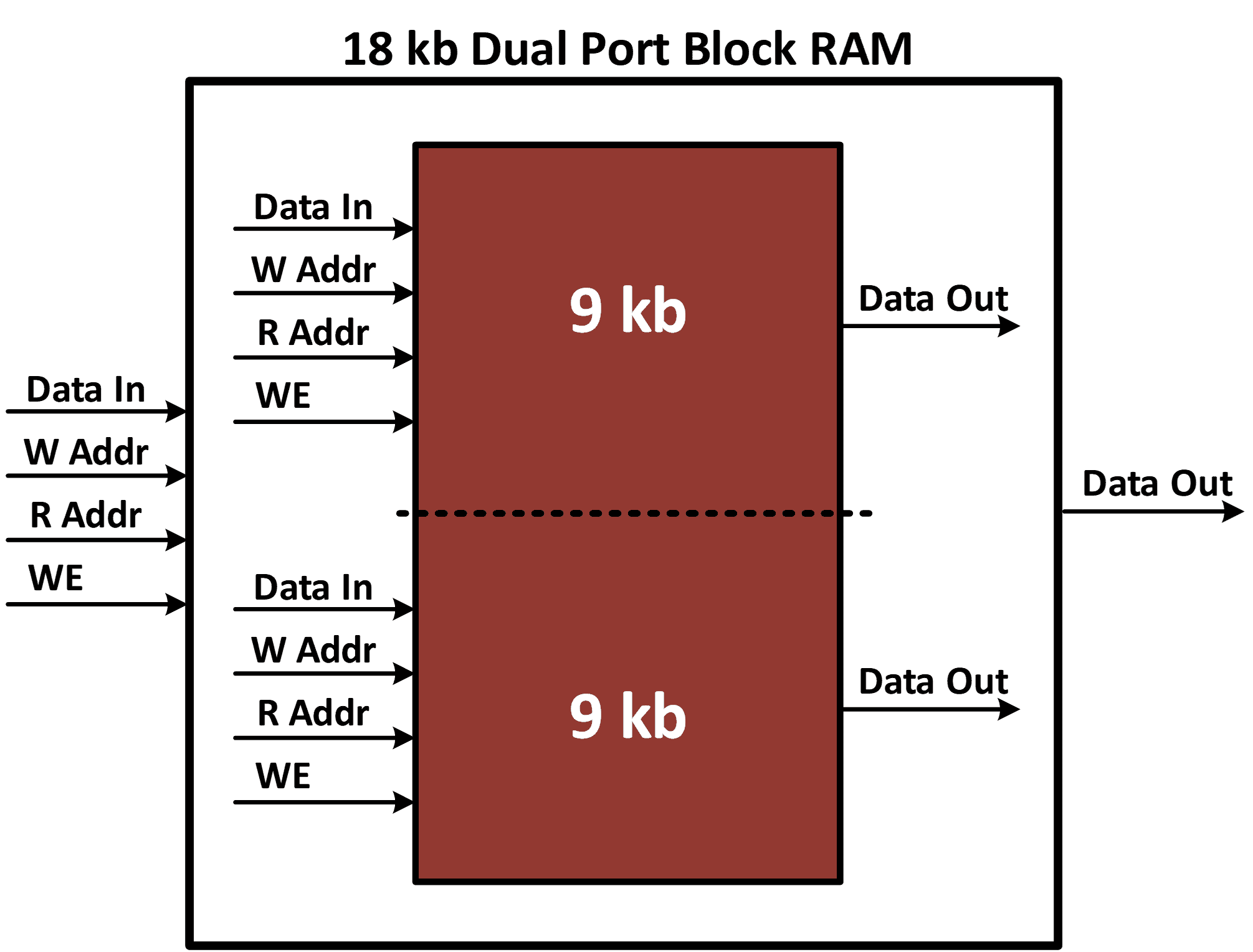
In this diagram, you can see an 18-kilobit Block RAM that has been divided into two 9-kilobit sections.

An 18-kilobit Block RAM that has been divided into two 9-kilobit sections.
If you need to, you can use the entire 18-kilobit memory at once using the port you see in this section. And if you need less than 9 kilobits of memory, you can use just 9 kilobits instead of the whole 18 kilobits.
Dual-Port Functionality and Memory Access Mechanisms:
Another point about Block RAMs is that they are dual-port memories. As you can see in this diagram, there are two independent ports for data input and output.
This means you can write data into the RAM through one port while simultaneously reading data from it through the other port.
Each of these ports has its own independent address line. For example, here we have a Write Address line and a Read Address line. There’s also a Write Enable input, which is used during the write operation.
For instance, if I want to write data into this memory, I first, place the data I want to write on the data input port, then specify the address where I want to write it on the Write Address line.
Finally, I activate the Write Enable port once to store the data at the desired location.
To read data from this memory, you simply place the desired address on the Read Address line. On the next clock cycle, the contents of that memory location will appear on the data output port.
Limitations and Considerations for Efficient BRAM Usage:
One last thing to note about Block RAMs is this:
if you use a portion of a Block RAM, such as allocating part of a 9-kilobit block to implement a 1-kilobit memory, and you need access to that 1-kilobit memory on every clock cycle, the rest of the 8 kilobits in that block will be unavailable for use.
This is because there's only one set of ports for this 9-kilobit memory.
So, if you use these ports to implement a 1-kilobit memory and you need to access the contents of that 1-kilobit memory on every clock cycle, you can't use the remaining 8 kilobits, and those 8 kilobits will essentially remain unused in the system.
Distributed RAM
Now, what are Distributed RAMs?
If you recall from previous articles, you know that every FPGA is made up of thousands of LUTs, or small memory units, which can be used to implement parts of your circuit.
By connecting these LUTs through the routing resources in the FPGA, you can design larger circuits. Some of these LUTs have the capability to be connected to each other and form a memory unit.
This memory, which is created by connecting LUTs, is called Distributed RAM.
How LUTs are Utilized to Create Distributed RAM:
One important point to note is that connecting these small LUTs to build a memory requires a significant amount of routing and additional circuitry in the FPGA.
In practice, when you create a Distributed RAM, a significant amount of FPGA resources are consumed.
Additionally, as the size of the Distributed RAM increases, the resource consumption grows exponentially. This severely limits the capacity of Distributed RAMs.
Note that the hardware resources used inside the FPGA to build Distributed RAMs could have been used to implement any other type of circuit if they weren't used for Distributed RAM.
Selecting the Right Memory: Block RAM vs. Distributed RAM
So, now you might be wondering: when should you use each type of memory? When should you use Block RAMs, and when should you use Distributed RAMs?
The answer to this question lies in the details I’ve already shared, but let me summarize the main points.
As I mentioned earlier, if you use a portion of a Block RAM and need constant access to it on every clock cycle, the rest of that memory block will go unused.
For example, if you only need 100 bits from a 9-kilobit Block RAM on every clock cycle, the remaining memory in that block will be unavailable.
This means that if you need very small memories, it’s not efficient to use Block RAMs for that purpose.
On the other hand, Distributed RAMs consume a lot of general-purpose resources, such as LUTs, when they are used to implement memory.
Connecting these LUTs requires extensive routing and additional components like multiplexers, which leads to even more resource usage.

Connecting the LUTs requires extensive routing and additional components like multiplexers in order to build Distributed RAMs.
This is something you'll see in practice when you use Distributed RAMs to implement temporary memory: as the size of the Distributed RAM increases, the various hardware resources in the FPGA are quickly consumed, and the FPGA fills up very quickly.
Another drawback of using Distributed RAMs for implementing larger memories is that the system’s clock speed will significantly decrease due to the way these memories are implemented. This can cause serious issues in your design.
Conclusion and Key Takeaways
So, in summary, the best time to use Distributed RAMs is when you need to implement very small memories—on the order of a few dozen to a few hundred bits.
And especially if you need to implement a large number of such small memories, that’s the best time to use Distributed RAM.
Block RAMs, on the other hand, are ideal for larger memories. For example, if you need 1 kilobit, 2 kilobits, or more, Block RAMs are the better option.
If you try to use Distributed RAMs for these larger memories, you’ll quickly see how fast the FPGA’s resources are consumed.
And another drawback is that because of the way these Distributed RAMs are implemented, when you implement a large memory, your system clock speed will also decrease significantly, and this can cause very serious problems for your system implementation.
Pro Tips!
The best time to use Distributed RAMs is when you need to implement very small memories.
Block RAMs, on the other hand, are ideal for larger memories.
Because of the way these Distributed RAMs are implemented, when you implement a large memory, your system clock speed will also decrease significantly


